
The last post about this project aimed at building a long-range camera remote control ended with a few working prototypes in need of a case. Designing such a case to be practical, good looking and easy enough to manufacture in small quantities proved to be way more complicated than I expected however, and it lead me back to the drawing board. Here is the story of how it went and the valuable lesson I learned along the way.
Where I got it wrong
When I started working on this project, I did what sounds logic at first to an electronics engineer (or at least to me) : I laid out the components on the PCB while at the same time giving some, but not much, thought to its integration in a case. Mainly, I put the buttons on the right side, the display on the left side, and tried to fit everything else on the smallest rectangular area possible around this. I didn’t have enough space for mounting holes so I thought I would make a snap-fit case. Anyway, this was tomorrow’s problem, right?
When tomorrow arrived I opened my favorite CAD software and tried a bunch of designs, but none of them really gave satisfaction. The snap-fit joints were not easy to 3D-print even on an SLA printer, and ended up being pretty fragile. Tolerances were hard to get right, and the top and bottom parts of the case would not align properly, even with lugs. In the top-right corner I couldn’t place a proper tab because of the antenna connector, leading to the case bending slightly near the top buttons (because of some misalignment) and exposing the PCB inside. I also tried a few designs for the buttons, either as separate parts or as flexible cutouts, but none of them really worked.
And overall, the case looked bulky and… ugly.
Besides the problems with making the case, other issues started to appear during these tests, with details I didn’t plan for at the beginning :
- all the connectors, especially the input and output 2.5mm jack connectors, were on the same side, and they were sometimes a bit too close to each other depending on the size of the cables that were plugged in
- the five navigation buttons on the right (up, down, left, right, center), even tough they appear gigantic when you are fully zoomed on your design on a 27″ monitor, felt in real life too small and too close to each other
- even though the breakout board of the OLED display was taking the full height of the board, the actual useful display area was actually off-centered (vertically) and looked too small as well
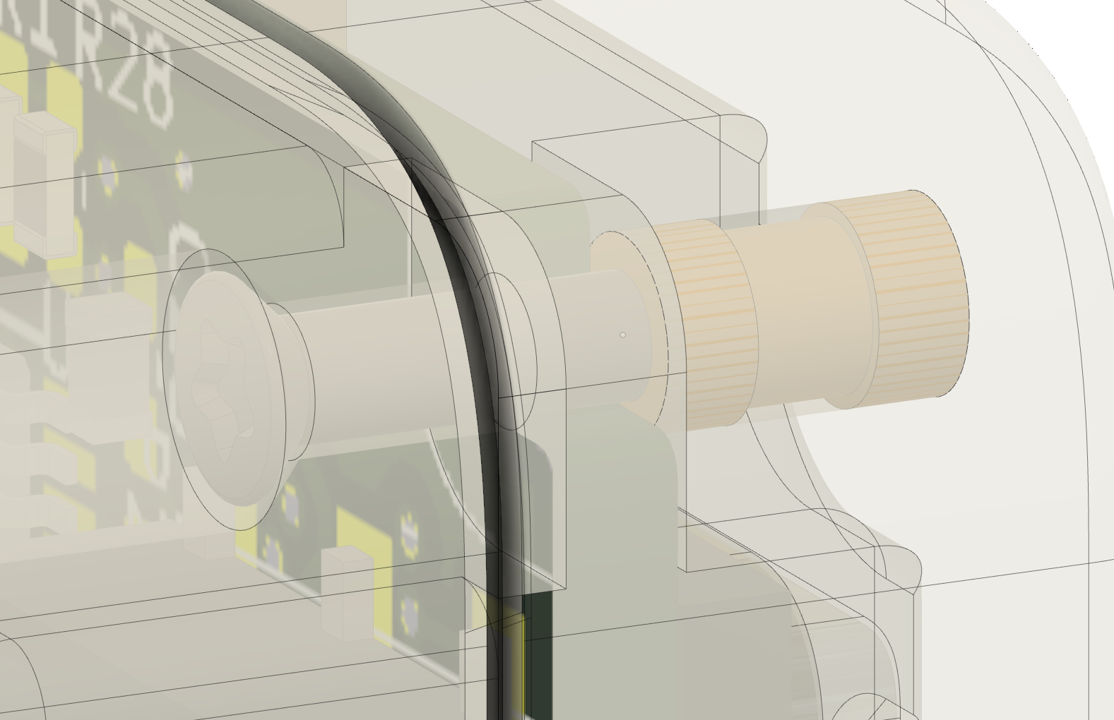
- the antenna connector sticked out of the board too much
- the two right-angle buttons at the top (power and trigger), next to the antenna, were more difficult to integrate, and were not confortable to reach for the user because of the antenna
- while testing the first prototypes I realized it would be great to be able to fix the receiver on the hotshoe at the top of the camera, but I didn’t have enough space to easily add such an anchor point

All of these details started to add up, until I was convinced that I needed to re-think my design from scratch.
Let’s pause and think about it
As I now realize, designing a small handheld device such as this one requires a tight integration between the electronics side and the mechanical side of the design. You can’t just make one of them and think about the other one later, you need to design both at the same time (which is certainly why professional ECAD and MCAD softwares tend to be more and more integrated to each other nowadays). I am by no means an expert on the subject and there will be nothing revolutionary exposed below, but here are a few personal takeaways from my experience with this project that you may find interesting.
Thinking as a user, not as an engineer
The user experience needs to be taken into account from the beginning.
When designing the first prototype I focused on the functional side of things : “Does the text appear on the screen? Does it react when I press the button? Great, it’s finished!”. But there is a completely different aspect of the problem that is equally important : is the screen large enough to be readable at the distance it will actually be used? Are the buttons wide enough and efficiently placed to instinctively fall under the thumb? Do they feel good to press? Is every external component (buttons, connectors, …) located somewhere which is both logical and practical from the user‘s point of view, instead of the layout‘s point of view?
For instance, when routing a layout it is sometimes instinctive to place connectors where they are easier to connect on the board, with shorter tracks and less zigzaging around. It may even offer better performances, when you consider high-speed signals or noisy high-power tracks. But a user (who might not even have seen a single PCB in their life) obviously doesn’t know or care about this sort of stuff, and expects to plug the cable where it makes sense to plug it. For example, it is usually more intuitive to find an input connector (power, data, …) on the left side, and an output connector (video output, actuators, …) on the right side.
This necessarily makes routing the board more difficult. However, you (and other people) will hopefully spend way more time using the device than you will spend working on this more complicated PCB design, making it well worth it in the end.
On a side note, when working with microcontrollers, a simple trick to make things easier at this stage is to identify what flexibility you have regarding GPIOs. During the development of the first prototype on a breadboard, GPIOs are usually assigned more or less at random, or at least for what makes sense for this particular implementation. But when designing the final schematic, it might be a good idea to make a list of the GPIO lines that are required without connecting them. Later in the layout stage, when the most important components (including the microcontroller) are placed and oriented on the board, the GPIO lines can be connected one by one in the schematic where it makes the most sense to minimize the layout complexity. You just need to remember to update the pin definitions in the firmware when you are done.
From the outside to the inside
Another point to think about from the beginning is the integration of everything (electronic or mechanic) that doesn’t necessarily appear on the layout but should be taken into account in the design. For instance, if an external component (battery, screen, …) is taped on one side of the board but the connector for it is on the other side, how the cables will fit in the case? It might be a good idea to add a notch in the outline of the PCB to route them cleanly. By the way, what is the actual length of cable available? If it is too short, a deeper notch might be necessary. If it is too long, moving the connector further away to cleanly “consume” the length of cable is a good option to consider. Thinking of the overall outside package and pushing things inside to fit everything will look better in the end than having to add protuberances or enlarge the whole case because of that one connector that sticks out of the board too much.


Adding mounting points is a pretty standard practice, but simply putting a 3mm hole at each corner of the board and hoping for the best is not always the best approach. Here are a few questions that might be worth considering :
- What size of screws (if using screws) is necessary? Mounting holes on off-the-shelf breakout boards are usually 3mm because M3 is a widespread standard, but could your design be strong enough with smaller (M2 or M1.6) screws, and would that make integration easier?
- Where can these mounting points be placed in order to not interfere with external components (both electronics and mechanical) while keeping the case rigid enough?
- Are screws really the best solution anyway? For example, maybe a notch on the board can fit into a corresponding notch in the case on the right side, while being locked into place on the left side by one of the screws for the case. This can be useful if there is no room for screws on the right side because of a large connector, or simply if you are running out of useful board area for routing components there.
- Do some external components on the board require additional mounting points? Even if this is not the case (assembled with double-sided tape, …), maybe they need some kind of lugs to make sure they are properly aligned during assembly.
- Is there enough clearance around every mounting point? Are there other areas where the board is in direct contact with the case which must be marked as “tracks but no component here” zones?
For example, here I saved some space by using M1.6 screws and only cutting a notch on each corner of the board instead of a closed circular hole. The PCB is sandwiched between the front and rear parts of the case, and the contact surface on both sides is marked on the silkscreen layer to make sure no component will be placed in the vicinity.
Another thing to take into account is the height of some components : connectors, some large capacitors or inductors, through-hole components… In order to make the integration as tight as possible, they must be placed somewhere they won’t interfere with another part above them. For instance, I wanted to ensure that the screen panel was as close to the PCB as possible in order not to waste space (which would have made the case thicker), therefore I had to make sure that no component under it was thicker than a 0603 capacitor. Ideally, if the height can be approximately consistent in this area, it might help the screen being level when assembled with double-sided foam tape.
Bottom line : all these considerations take space on the board and add lots of constraints on the layout, making routing more difficult. However, it will probably still be easier than having to deal with integration issues later.
Now, doing it right
In order to solve all these issues, I decided to completely change my workflow and start with the mechanical design first.
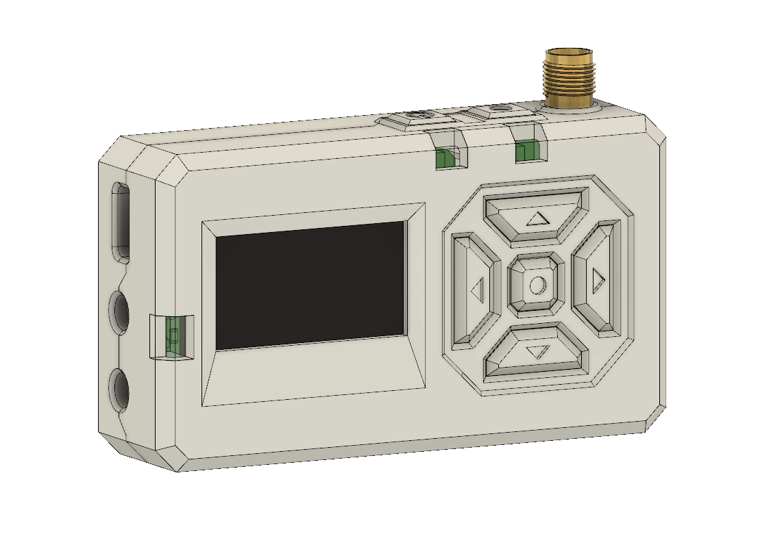
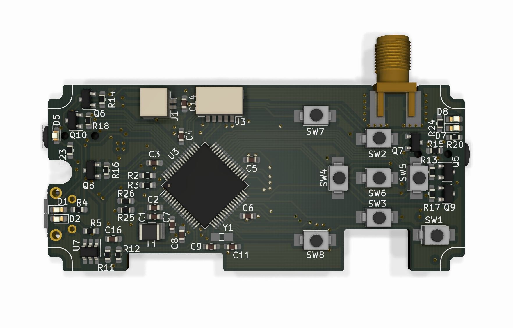
I found a larger screen panel on buydisplay.com (a 1.3″ one with a flat cable connector, no breakout board this time), made a 3D model of it, and placed larger buttons to its right, all of them on the front side. I then placed the connectors and their associated LEDs where it made sense, and added the hotshoe support. Finally, I designed a case around that and tried to make it better looking than before.
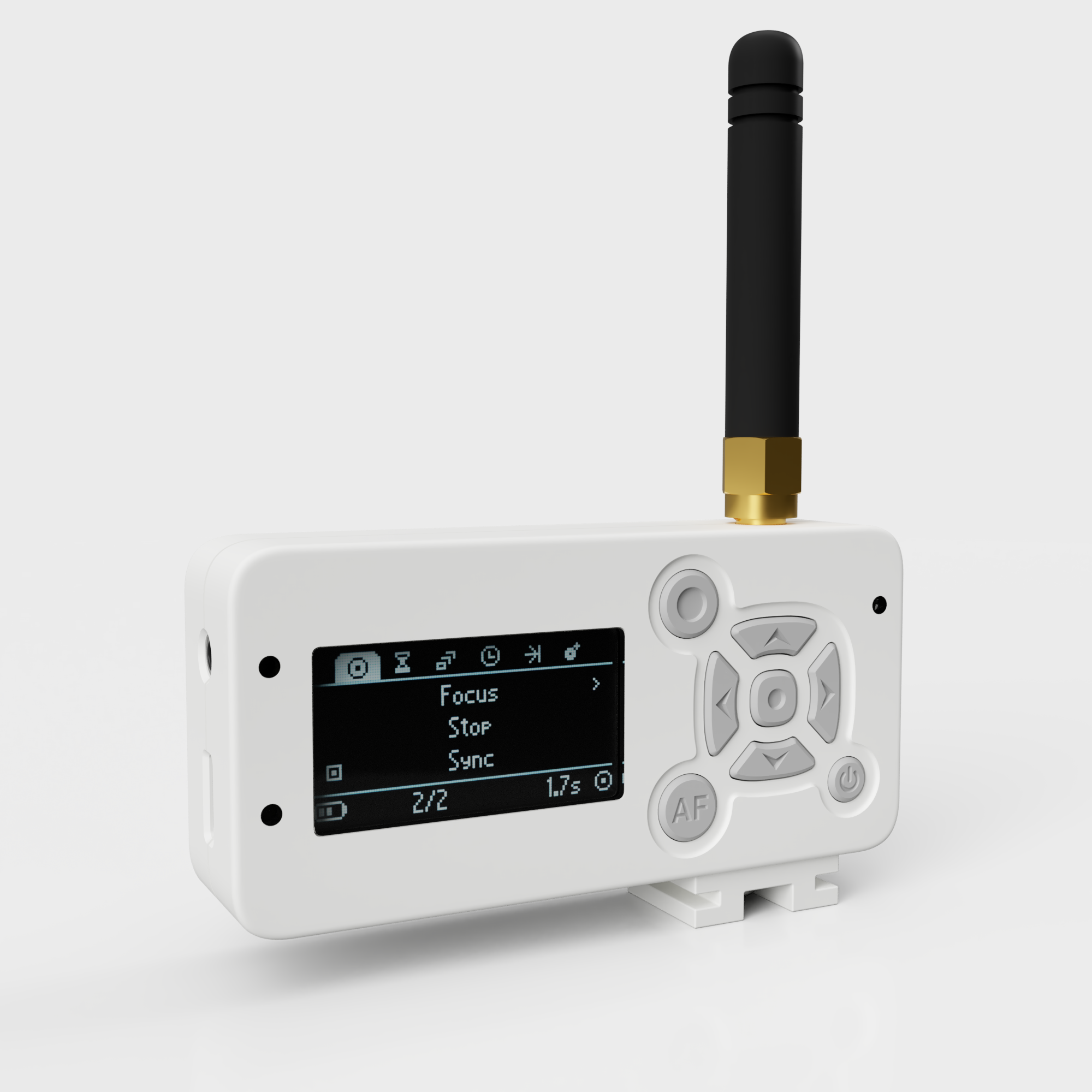
A few iterations were 3D-printed to make sure it felt good in hands.
Now that it looked good on the outside, I worked on fitting everyting inside. I added a PCB in the 3D model with cutouts to accomodate the components already in place, then the other bigger components, such as the battery.
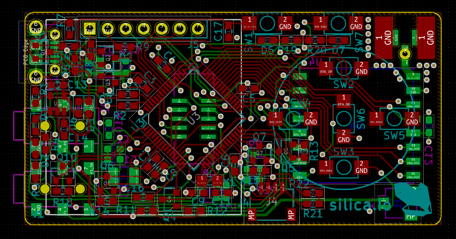
When I was satisfied with this model, I simply exported the board profile as a DXF and imported it inside Kicad on the board outline (Edge.Cuts) layer.

I then placed every “fixed” component (connectors, buttons, LEDs, …) on the layout according to their position in the 3D model (by manually measuring and moving the components one by one, unfortunately I didn’t find a way to automate this step), isolated the components and areas with height constraints (mainly the internal connector for the battery), and added silkscreen markings for the clearances around the mouting points.
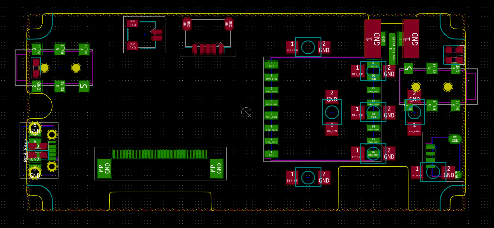
Finally, placing and routing the rest of the components was business as usual.


I exported the 3D model in STEP format from Kicad and imported it into Fusion. This allowed me to check that there was no conflict between parts and that everything fit perfectly inside the case. By the way, if you are using Kicad and FreeCAD, there are plugins for the latter that allow seemless synchronization between both.
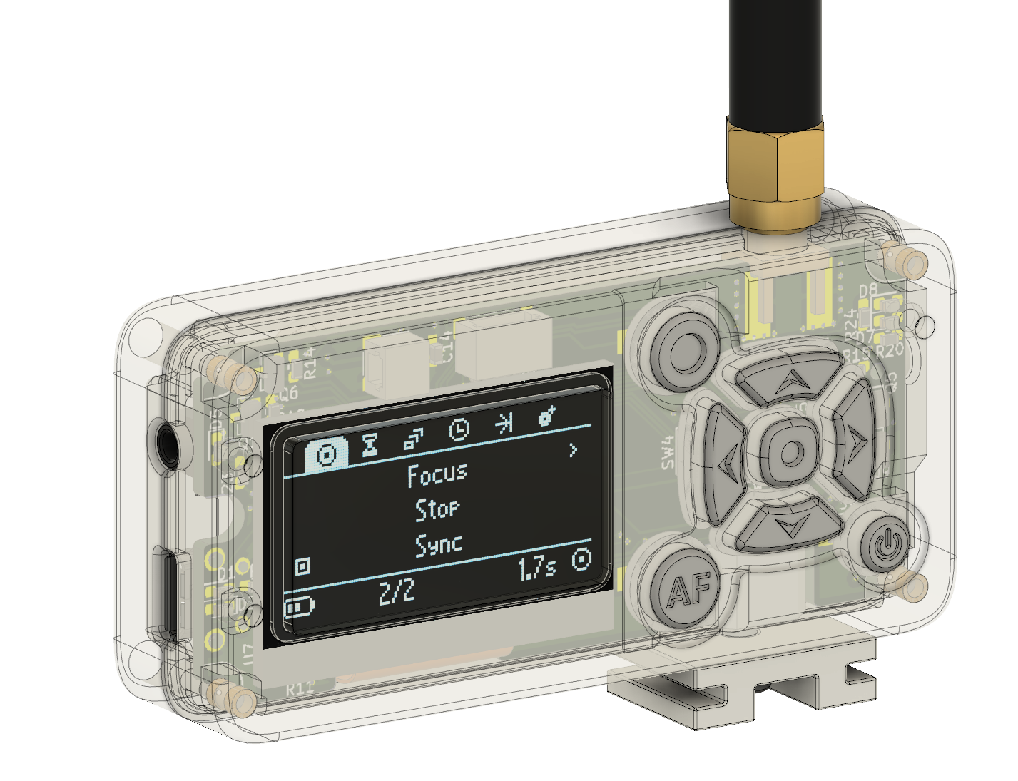
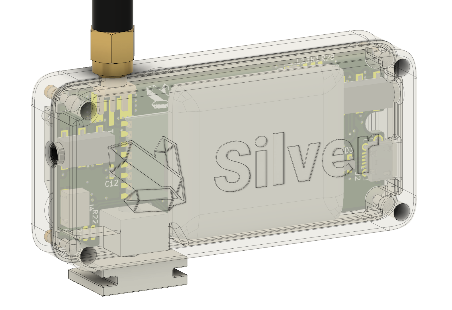
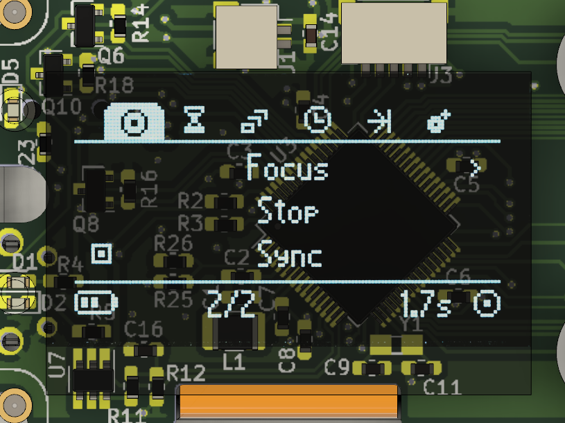
As usual, OSHPark skillfully transformed the design into cute purple boards, which I promptly assembled by hand. I updated the firmware to account for these modifications on the board, and added a few features at the same time, such as a footer (which can be seen in the renders above) with the battery gauge and the progress of the intervallometer.
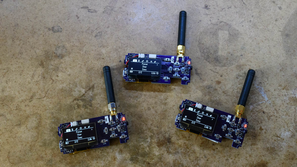
Time to make the cases. I 3D-printed some of them on my Form2, but I also had a set printed in white PA12 Nylon (with an SLS printer) by Sculpteo to see how it would compare (I will talk more about the exact reason in a later post).
I battle-tested these prototypes at this year’s C’Space, during which I used them intensively for 5 days to capture launches of experimental rockets.
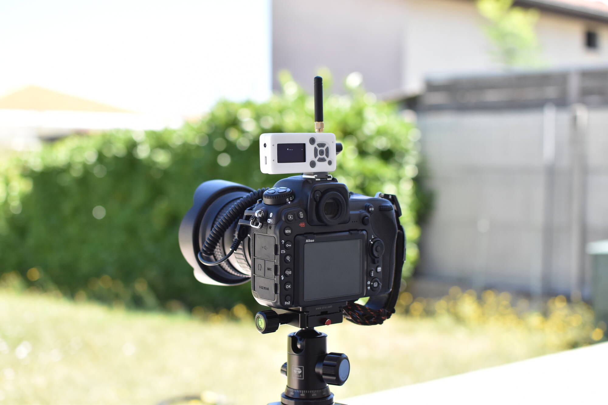
My set up during the event was slightly complicated and proved the versatile capabilities of these modules. I had my two cameras on the launchpad, usually one at 11mm (wide angle) shooting the ramp and the sky and the other one at 35mm (tighter frame) shooting the rocket exiting the ramp. Both of them had a Silver connected to them, while I had the third one in my hand acting as the remote control. The IR sensor fixed on the ramp to detect the launch was used as a backup and plugged into the input port of one of the modules on the launchpad. This way I could trigger the burst of photos manually using the remote, but in case I forgot (or if the radio packet lost itself in the air), the sensor automatically triggered the first receiver which then triggered the other one by radio.


Overall, I’m very happy with the result. I am now experimenting with different manufacturing methods for the case, but this is still very much a work in progress and will be the subject of a later post.
Remote camera capability for capturing rocket launches is exactly what I’m needing. I would be interested in several units if you do production.
Hi Jim,
Thanks for your feedback and interest, I’ll make sure to let you know when I build more of them.
Best,
Wow! It’s not something I really need, but something I would love to build and try out! Seeing as I love photography and diy electronics. I hope you do a run on tindie!
Hey there Foaly, I’ve been searching for long range camera triggering solutions for a little while now for an upcoming backcountry snowboard film project i’ll be working on. I was resigned to attempting to design something myself but you’ve already gone ahead and eloquently developed something super nice!
Are you planning on going into production soon? I’m looking for a couple units to be used in adverse weather (high humidity, -20c blizzarding conditions)
I’d be grateful for a chat if you have some spare time
Hi Torin,
Thanks for your interest. Currently I am actively working on finishing the casing for the module (you can find some recent photos here : https://hackaday.io/project/167218-silver) and performing more performance and reliability tests, then I am indeed planning for a small prototypes batch (probably around 10 units) to propose to some interested users in the comments. I will be contacting you as soon as everything is ready, which should be around december or january if everything goes as planned.
Your requirement for adverse weather is interesting : I will look into it and try to do some testing.
In the meantime if you want to chat feel free to contact me by email : use my username (f…y) followed by @silica.io.
Great learning experience. You found the holistic approach is key when both the electronics and mechanicals will end up in the real world. One recommendation for your work flow. Give the kicad stepup integration for kicad to FreeCAD. Avoids the need for the dxf, allows bidirectional pcb shape design, and direct 3d pcb to FreeCAD.
Thanks for the feedback. Indeed, I definitely need to switch to FreeCAD in the future (especially following the latest changes to Fusion licenses). I just couldn’t get used to it the few times I tried it and I couldn’t afford the time it would take at the moment, but the integration with Kicad will definitely be a motivation for it.
Great write-up, just wish I had read it a couple of years ago to avoid making the same mistakes 🙂
Was going to add to watch out for recent Fusion 360 license changes and to at least consider another CAD program. But I see I’m not the only one that has been impacted by their recent license changes. It took me over a month and a lot of online chatting and emailing to get my startup license renewed. Since I use KiCAD extensively, I’ve used this ‘opportunity’ to start transitioning to FreeCAD and stepup. Painful at first but I’m liking it more the longer I use it.
Thanks!
I haven’t looked closely at those licenses yet, as I haven’t opened Fusion since then, but your experience makes me look forward to it even less. I will try to “port” this design to FreeCAD as a training, and hopefully I will have the same feeling as you in the end. Kicad in its own way is also not always user-friendly at first, but now I wouldn’t use anything else.
“I then placed every “fixed” component (connectors, buttons, LEDs, …) on the layout according to their position in the 3D model (by manually measuring and moving the components one by one, unfortunately I didn’t find a way to automate this step)”
How about placing some tiny holes (0.1mm) at the center of each button/LED in Fusion360, which get exported together with the board outline? You can then easily align the components in KiCad, and delete the hole contours from the Edge.Cuts layer afterwards?
That’s a great idea! As discussed in the other comments I might go up a different route and switch to FreeCAD which shouldn’t require such a trick thanks to its integration with Kicad, but it’s still a useful trick to remember and it might help others using other CAD software.
Thanks for sharing!
Happy to help! Your final design is fantastic. I hope to build some new enclosed PCB projects in the future.
As a Mechanical Engineer who’s used to SolidWorks & co., and using Fusion360 for hobby projects, I’m still reluctant to switch to FreeCAD. I feel like the functionality, speed of development and stability are still not there yet for everyday use, especially for assemblies consisting of more than 2~3 parts… Happy to be proven wrong with a future post of yours!
So, I’ve given FreeCAD a try by making (most of) the top part of the case.
After speding a bit of time to learn the basics, it went better than I expected. Some advanced features are surprisingly powerful (such as the handling of B-splines or the spreadsheet workbench), while some other, basic features are surprisingly missing (such as some sketch constraints, using external geometry directly in a sketch, or making a chamfer that would delete a face). The UI is sometimes not very user-friendly (such as when it asks you to select a feature by finding its name in a pop-up list, instead of clicking on it in the 3D view) but still usable if you don’t mind spending a bit more time on your project. I haven’t used any Assembly feature, and no assembly workbench is provided by default, but the A2Plus plugin seems to work well from what I saw on Youtube.
https://silica.io/wp-content/uploads/2019/12/freecad_test.png
I’ve experienced a few crashes, but nothing too bad since FreeCAD was able to restore my file every time. The only hair-pulling moment was when I tried to move a feature in the history tree, which FreeCAD didn’t like at all because of dependency issues but tried to do anyway, and that completely broke every feature below this one in my history tree. “Undo” was unable to fix this, in the end I had to delete all these features and draw them again.
Overall I’d say it’s still a bit rough around the edges, and I think even with similar experience it would still be significantly longer to do the same part on FreeCAD than it would on SolidWorks/Fusion360. But given the fact that FreeCAD is free and open-source, it’s an incredible, very capable software, especially for hobbyists that do not think in terms of hourly rates. It looks like development is very active with lots of fixes and new features added in the past years, so I’m looking forward to future updates and I will try and see if I can implement some of the simpler missing features myself. In the meantime, this test proved that in its current state FreeCAD is good enough for most of my needs so I will continue using it for any new MCAD project that comes my way.
Let me know if you decide to put these on Tindie. I’d take a set. with regards to the Fusion 360 discussions above, I will say that Autodesk could have handled this better. I’m still using the free version and have done so with no interruption of service. BUT, I did loose the ability to import/export many file versions, most notably, Solidworks .sldprt files, though I can still import/export .step files. Also, getting files out of the online shared workspace has been a PITA. But even with all that, there is still noting that compares. Plus I also need CAM from time to time so having that is nice too. I wouldn’t give up on it.
I’ve also spent some time with Freecad and I agree, its not bad for smaller designs. But for larger, more complicated designs, there are significant shortcomings. Speed becomes a real problem. I’ve also had issues with the exported .step files from Freecad. Some work fine with Solidworks or Fusion, others do not, and I was not able to determine the cause.
Hi John, thanks for your interest. I will contact you as soon as I have modules available.
Indeed, those issues sound like a pain. It’s a shame Fusion is taking such a path, even though having such a powerful software for free is amazing in the first place. Hopefully, the development of Freecad will continue and the software will eventually reach the point of usability that Kicad currently offers for ECAD.
Hi, what’s the power consumption of the receiver and how big is the latency between pressing the remote’s button and triggering the camera?
Hi,
I don’t have precise measurements on hand but I’d say respectively around 10mA and 1/10th of a second
Hi, I just read about this long distance triggering project which is very interesting. I was trying to find a trigger for my camera with such capabilities. Do you already have some production units to test? Can we find somewhere the project roadmap?
Thank you for such good job!
Hi,
Thanks for your interest. I have a few prototypes in need of a case; unfortunately I don’t have a precise roadmap right now but I’m working on it. Thanks for your patience !
Thanks to you. I will stay tunned to your project and hopefully we will be able to get a sample unit soon. This seems to fit perfectly to my photography needs.
I too am interested in this project. I don’t have the time or skills to build. Please add me to your list if you ever want to sell one. My interest is outdoor photography.
I would also purchase a few if your ever make a production run.
What’s the current status of this project? I’d be interested.
Hiya Foaly, Nice Work on your Project, I am a Photographer, and do quite a few custom DIY improvisations to get image capture & lighting, some experience in multi-cam, I am super keen to know, if/when you have any of these units available. I wanted to suggest… if its useful for you… can get a cheap reversing camera monitor, and 5.8 Ghz radio gear for video signal, (just in analog) and if it useful, you can see the cams LCD photo output on screen from a distance, im working on how to toggle between cams with this 5.8 system (i shoot six cams) and also controlling lighting, would be great to have a chat via email, im considering using Heltec LoRa units. Be great to hear from you via email
Hello, it’s been a while since you posted any updates on this but looks like what I need.
Do you have files for the case available, and did you get it working to satisfaction with the last updates? Do you know if anyone else has successfully built these?
This would be great for an idea I have to photograph much larger sized rockets… I would like to control like 20 cameras in sequence. would greatly appreciate any sort of input you have now
Hi Jason,
This project has been put on hold for now mainly due to parts shortage (especially the microcontroller), however, I’ve used the few prototypes that I have for rocket launches this summer and everything worked as expected.
It should work fine for 20 cameras, and you can configure independent delays on each receiver to set up the sequence that you would like. Is there any special feature that you would need for this purpose?
I’ll post an update here when there is news regarding the possibility of a larger production batch.
Hi Foaly,
this seems to be a great project to trigger remote dslrs on equipment like drones for photogrammetry, I was looking at the github files but I was wondering if ever started production or if you are going to make the files available to order assembled boards.
It is a very cool project, looking forward to hear from you.
Hey Foaly,
Did you ever make more of these or do you have a full parts list? I had commented on your original blog, but it seems you made quite a few enhancements. I’ve been using my old Arduino based project I made years ago again to remote trigger cameras for some vintage aircraft filming, but I’m having quite a few reliability issues with it and would love to give yours a try rather than attempt to fix my very dumb solenoid system. I’m happy to make them myself or buy a couple if you have any around.
Foaly,
I started building this board from parts that I ordered years ago. I don’t know if the case was available for order from Sculpteo back in the day, but the link returns 404. Is it possible to get STLs for the case? I looked around on GitHub and didn’t see them.
Thanks